We’ve been hearing about NVIDIA’s Kepler architecture since about September 2010. It was back at that years’ NVIDIA GPU Technology Conference, that company CEO Jen-Hsun Huang first publically disclosed that Kepler would offer massive performance per watt improvements over Fermi and previous-gen architectures and that GPUs based on Kepler would arrive in 2011. Well, the launch date has obviously slipped. How Kepler’s power efficiency looks, we’ll get to a little later.
The rumor mill kicked into high gear over the last few months, and has been consistently churning out more and more Kepler scuttlebutt (whether true or false) coincident with Radeon HD 7000 series launches. Today though, we can put the rumors to rest. We’ve had a new Kepler-based GeForce GTX 680 in hand for a couple of weeks now and can finally reveal all of the juicy details.
First up, we have some specifications and a little back story. And on the pages ahead, we’ll dive a little deeper and give you all the full scoop on Kepler, its new features and capabilities, and of course the GeForce GTX 680’s features and performance.
The NVIDIA GeForce GTX 680, GK104 "Kepler" Based Graphics Card
|

The GeForce GTX 680’s main features and specifications are listed in the table above. Before we get into the specifics of the card and it’s GPU, however, we want to direct your attention to a few past HotHardware articles that lay the foundation for what we’ll be showing you here.

GK104 "Kepler" GPU Die Shot
As we’ve mentioned, the GK104 GPU powering the GeForce GTX 680 is based on NVIDIA’s new Kepler architecture. Kepler, however, is not a complete redesign from the ground up. Although much more power efficient and higher performing than Fermi using a number of key metrics, Kepler does borrow heavily from Fermi’s design.

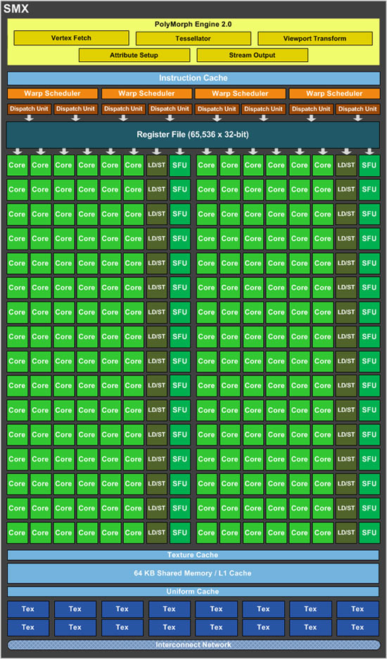
NVIDIA GK104 GPU Block Diagram
The high-level block diagram above shows the overall structure on the GK104. The chip has an arrangement of four Graphics Processing Clusters (GPC), each with two Streaming Multiprocessors, dubbed SMX (a Streaming Multiprocessors in Fermi is called a SM). Within each GPC, there is control logic, plus 192 CUDA cores, for a total of 1536 CUDA cores per GPU. In the previous-gen GTX 580 (Fermi), there were 32 CUDA cores per SM, which were duplicated 16 times within the chip. With the GK104, there are 192 CUDA cores per SMX, which are duplicated 8 times. The structure results in 6x the number of cores per SM(X) and 3x the total number of cores than the GeForce GTX 580.
A Close-Up Of A Single SMX In The GK104 GPU
In terms of its other features, the GK104 has a total of 128 texture units and 32 ROPs. There is 512K of L2 cache on-die, and the GPU interfaces with the GeForce GTX 680’s 2GB of GDDR5 memory over a 256-bit interface. It supports DirectX 11 (not 11.1) and features a PCI Express 3.0 host interface. There are eight geometry units in the chip (Polymorph Engine 2.0) and four raster units (one per GPC). According to NVIDIA, the Polymorph 2.0 engines offer double the primitive and tessellation performance per SM of Fermi.
In addition to having a different GPC and SM arrangement, with Kepler, NVIDIA also minimized the hardware control logic in the chip to bring the transistor count down and Kepler will also operate with a single clock domain—shaders/CUDA cores are not clocked at 2x the frequency of the rest of the chip.
With the GK104, the sum total of all of these changes is a 3.54 billion transistor chip with a die size of about 294 square mm, which is manufactured using TSMC’s 28nm process node. If you’re keeping track, that’s about 770M fewer transistors than AMD’s Tahiti GPU in the Radeon HD 7900 series and a significantly smaller die size (294mm2 vs 365mm2) as well.

The GeForce GTX 680 performed very well in Futuremark's 3DMark11 benchmark as well. Here, the GeForce GTX 680 outpaced the Radeon HD 7970 by about 16.6% and the GeForce GTX 580 by over 50%. The only cards that were able to outrun the GeForce GTX 680 in 3DMark11 were the dual-GPU powered GeForce GTX 590 and Radeon HD 6990.
Before bringing this article to a close, we'd like to cover a few final data points--namely power consumption and noise. Throughout all of our benchmarking and testing, we monitored acoustics and tracked how much power our test system was consuming using a power meter. Our goal was to give you an idea as to how much power each configuration used while idling and while under a heavy workload. Please keep in mind that we were testing total system power consumption at the outlet here, not just the power drawn by the graphics cards alone.

The new GeForce GTX 680 proved to be quite power friendly under both idle and load conditions. With the GeForce GTX 680 idling at the Windows desktop (with the monitor displaying an image) out test machine consumed only 122 watts—11 watts fewer than the GeForce GTX 580 and 5 watts fewer than the Radeon HD 7970.
With the GeForce GTX 680 loaded up, our test system’s power consumption jumped up to only 358 watts, which was among the lowest of the bunch. When running under load conditions, the GeForce GTX 680 consumed 46 fewer watts than the GeForce GTX 580 and 17 fewer watts than the Radeon HD 7970. That’s a big win for NVIDIA after years of more power efficient AMD GPUs.
With the improvements made to the GeForce GTX 680’s PCB and cooling hardware and the power efficiencies inherent to the architecture, it should come as no surprise that the GeForce GTX 680 runs relatively cool and quiet. Our particular card idled at about 42’C and peaked at about 73’C under load according to EVGA’s Precision utility.
Noise was also a non-issue. At idle, the GeForce GTX 680 is essentially silent and couldn’t be heard above the noise produced by our CPU cooler and PSU. Under load, the card’s fan did spin up to audible levels, but we would not consider the card loud by any means.
Performance Summary: NVIDIA made summarizing the GeForce GTX 680’s performance nice and easy. To put it simply, the GeForce GTX 680 is the fastest single-GPU based graphics card we have tested to date. Generally speaking, the GeForce GTX 680 was between approximately 5% and 25% faster than AMD’s Radeon HD 7970, depending on the application. Although, the Radeon HD 7970 was able to pull ahead in a couple of spots, like Alien vs. Predator. In comparison to NVIDIA’s previous single-GPU flagship, the GeForce GTX 580, the new GTX 680 is between 15% and 50% faster. Versus ultra high-end, dual-GPU powered cards like the Radeon HD 6990 and GeForce GTX 590, the GeForce GTX 680’s performance still looks good, as it was able to outrun those dual-GPU powerhouses on a few occasions.

NVIDIA GK104 GPU Block Diagram
The high-level block diagram above shows the overall structure on the GK104. The chip has an arrangement of four Graphics Processing Clusters (GPC), each with two Streaming Multiprocessors, dubbed SMX (a Streaming Multiprocessors in Fermi is called a SM). Within each GPC, there is control logic, plus 192 CUDA cores, for a total of 1536 CUDA cores per GPU. In the previous-gen GTX 580 (Fermi), there were 32 CUDA cores per SM, which were duplicated 16 times within the chip. With the GK104, there are 192 CUDA cores per SMX, which are duplicated 8 times. The structure results in 6x the number of cores per SM(X) and 3x the total number of cores than the GeForce GTX 580.
A Close-Up Of A Single SMX In The GK104 GPU
In terms of its other features, the GK104 has a total of 128 texture units and 32 ROPs. There is 512K of L2 cache on-die, and the GPU interfaces with the GeForce GTX 680’s 2GB of GDDR5 memory over a 256-bit interface. It supports DirectX 11 (not 11.1) and features a PCI Express 3.0 host interface. There are eight geometry units in the chip (Polymorph Engine 2.0) and four raster units (one per GPC). According to NVIDIA, the Polymorph 2.0 engines offer double the primitive and tessellation performance per SM of Fermi.
In addition to having a different GPC and SM arrangement, with Kepler, NVIDIA also minimized the hardware control logic in the chip to bring the transistor count down and Kepler will also operate with a single clock domain—shaders/CUDA cores are not clocked at 2x the frequency of the rest of the chip.
With the GK104, the sum total of all of these changes is a 3.54 billion transistor chip with a die size of about 294 square mm, which is manufactured using TSMC’s 28nm process node. If you’re keeping track, that’s about 770M fewer transistors than AMD’s Tahiti GPU in the Radeon HD 7900 series and a significantly smaller die size (294mm2 vs 365mm2) as well.
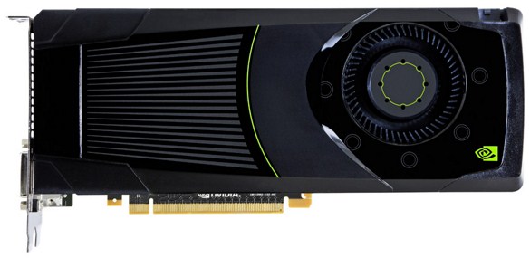
On the surface, the new GeForce GTX 680, looks much like it’s brethren in the GeForce GTX 400 and 500 series, but there are many changes introduced at the board level as well. The GeForce GTX 680’s cooler sports a number of new features too.

The NVIDIA GeForce GTX 680 Graphic Card - Front and Back
Let’s get the specifications covered first. Reference GeForce GTX 680 cards will have a base GPU clock speed of 1006MHz, with a Boost clock of 1058MHz. If you’re asking yourself what a “Boost clock” is, don’t fret, we’ll cover that on the next page—for now, just think of it as Turbo Boost for GPUs. GeForce GTX 680 cards will have 2GB of GDDR5 memory, linked to the GPU over a 256-bit interface, with an impressive 6008MHz effective data rate. The result is a peak of 192.26GB/s of memory bandwidth. And the GeForce GTX 680’s peak texture fillrate is 128.8GT/s.
Based on NVIDIA’s track record the last few years, you may think that a card that’s seemingly as powerful as the GeForce GTX 680 requires a ton of power, but that’s not the case. Reference GeForce GTX 680s have a TDP of “only” 195 watts and require a pair of 6-pin PCI Express power connectors. For reference, the GeForce GTX 580 has a TDP of 244 watts.


The GeForce GTX 680's Cooler and GPU Exposed
Despite having lower power requirements, NVIDIA still put significant resources into keeping the GeForce GTX 680 cool and quiet. The fan on the GeForce GTX 680’s cooler reportedly features acoustic dampening material which lowers its pitch and minimizes whine. The heatsink itself features a densely packed array of aluminum fins with a high-efficiency embedded heatpipe and heavy copper base to more efficiently wick heat from the GPU. And the heatsink is cut at an angle and pushed back from the case bracket to allow air to more easily pass through the heatsink and escape through the vents in the bracket. The end result is a card that’s quieter than the GeForce GTX 580, which we found to run relatively cool as well.

The GeForce GTX 680's Case Bracket and Outputs
In terms of its output configuration, the GeForce GTX 680 has two DL-DVI outputs, a single HDMI 1.4a output (with 4K monitor support), and a single DisplayPort 1.2 output. But more importantly, the cards support up for four active displays—previous GeForces could only run two displays simultaneous. Being able to power four displays means the GeForce GTX 680 can power multi-monitor 3D Vision Surround setups from a single card.
How We Configured Our Test Systems: We tested the graphics cards in this article on an Asus P9X79 Deluxe motherboard powered by a Core i7-3960X six-core processor and 16GB of G.SKILL DDR3-1600 RAM. The first thing we did when configuring the test system was enter the system UEFI and set all values to their "optimized" or "high performance" default settings and disabled any integrated peripherals that wouldn't be put to use. The hard drive was then formatted and Windows 7 Ultimate x64 was installed. When the installation was complete we fully updated the OS and installed the latest DirectX redist, along with the necessary drivers, games, and benchmark tools.


The new GeForce GTX 680 kicked some major tail in the Unigine Heaven benchmark. NVIDIA's latest flagship put up scores about 23% higher than the Radeon HD 7970 and 49% higher than the GeForce GTX 580. Only the dual-GPU powered GeForce GTX 590 was able to put up a higher score and even then it was only buy a couple of percentage points.
The NVIDIA GeForce GTX 680 Graphic Card - Front and Back
Let’s get the specifications covered first. Reference GeForce GTX 680 cards will have a base GPU clock speed of 1006MHz, with a Boost clock of 1058MHz. If you’re asking yourself what a “Boost clock” is, don’t fret, we’ll cover that on the next page—for now, just think of it as Turbo Boost for GPUs. GeForce GTX 680 cards will have 2GB of GDDR5 memory, linked to the GPU over a 256-bit interface, with an impressive 6008MHz effective data rate. The result is a peak of 192.26GB/s of memory bandwidth. And the GeForce GTX 680’s peak texture fillrate is 128.8GT/s.
Based on NVIDIA’s track record the last few years, you may think that a card that’s seemingly as powerful as the GeForce GTX 680 requires a ton of power, but that’s not the case. Reference GeForce GTX 680s have a TDP of “only” 195 watts and require a pair of 6-pin PCI Express power connectors. For reference, the GeForce GTX 580 has a TDP of 244 watts.
The GeForce GTX 680's Cooler and GPU Exposed
Despite having lower power requirements, NVIDIA still put significant resources into keeping the GeForce GTX 680 cool and quiet. The fan on the GeForce GTX 680’s cooler reportedly features acoustic dampening material which lowers its pitch and minimizes whine. The heatsink itself features a densely packed array of aluminum fins with a high-efficiency embedded heatpipe and heavy copper base to more efficiently wick heat from the GPU. And the heatsink is cut at an angle and pushed back from the case bracket to allow air to more easily pass through the heatsink and escape through the vents in the bracket. The end result is a card that’s quieter than the GeForce GTX 580, which we found to run relatively cool as well.
The GeForce GTX 680's Case Bracket and Outputs
In terms of its output configuration, the GeForce GTX 680 has two DL-DVI outputs, a single HDMI 1.4a output (with 4K monitor support), and a single DisplayPort 1.2 output. But more importantly, the cards support up for four active displays—previous GeForces could only run two displays simultaneous. Being able to power four displays means the GeForce GTX 680 can power multi-monitor 3D Vision Surround setups from a single card.
How We Configured Our Test Systems: We tested the graphics cards in this article on an Asus P9X79 Deluxe motherboard powered by a Core i7-3960X six-core processor and 16GB of G.SKILL DDR3-1600 RAM. The first thing we did when configuring the test system was enter the system UEFI and set all values to their "optimized" or "high performance" default settings and disabled any integrated peripherals that wouldn't be put to use. The hard drive was then formatted and Windows 7 Ultimate x64 was installed. When the installation was complete we fully updated the OS and installed the latest DirectX redist, along with the necessary drivers, games, and benchmark tools.
|
| Hardware Used: Intel Core i7-3960X (3.3GHz, Six-Core) Asus P9X79 Deluxe (Intel X79 Express) Radeon HD 7950 Radeon HD 7970 Radeon HD 6970 GeForce GTX 580/OC GeForce GTX 580 3GB GeForce GTX 590 GeForce GTX 680 16GB OCZ DDR3-1600 Western Digital Raptor 150GB Integrated Audio Integrated Network | Relevant Software: Windows 7 Ultimate x64 DirectX April 2011 Redist ATI Catalyst v12.2b NVIDIA GeForce Drivers 300.99 Benchmarks Used: Unigine Heaven v2.5 3DMark 11 Batman: Arkham City Just Cause 2 Alien vs. Predator Metro 2033 Lost Planet 2 Dirt 3 |
|
 Unigine Heaven | Unigine's Heaven Benchmark v2.5 is built around the Unigine game engine. Unigine is a cross-platform, real-time 3D engine, with support for DirectX 9, DirectX 10, DirectX 11 and OpenGL. The Heaven benchmark--when run in DX11 mode--also makes comprehensive use of tessellation technology and advanced SSAO (screen-space ambient occlusion) It also features volumetric cumulonimbus clouds generated by a physically accurate algorithm and a dynamic sky with light scattering. |
The new GeForce GTX 680 kicked some major tail in the Unigine Heaven benchmark. NVIDIA's latest flagship put up scores about 23% higher than the Radeon HD 7970 and 49% higher than the GeForce GTX 580. Only the dual-GPU powered GeForce GTX 590 was able to put up a higher score and even then it was only buy a couple of percentage points.
Futuremark 3DMark11
|
Synthetic DirectX Gaming
|
 Futuremark 3DMark11 | The latest version of Futuremark's synthetic 3D gaming benchmark, 3DMark11, is specifically bound to Windows Vista and WIndows 7-based systems due to its DirectX 11 requirement, which isn't available on previous versions of Windows. 3DMark11 isn't simply a port of 3DMark Vantage to DirectX 11, though. With this latest version of the benchmark, Futuremark has incorporated four new graphics tests, a physics tests, and a new combined test. We tested the graphics cards here with 3DMark11's Extreme preset option, which uses a resolution of 1920x1080 with 4x anti-aliasing and 16x anisotropic filtering. |
The GeForce GTX 680 performed very well in Futuremark's 3DMark11 benchmark as well. Here, the GeForce GTX 680 outpaced the Radeon HD 7970 by about 16.6% and the GeForce GTX 580 by over 50%. The only cards that were able to outrun the GeForce GTX 680 in 3DMark11 were the dual-GPU powered GeForce GTX 590 and Radeon HD 6990.
Before bringing this article to a close, we'd like to cover a few final data points--namely power consumption and noise. Throughout all of our benchmarking and testing, we monitored acoustics and tracked how much power our test system was consuming using a power meter. Our goal was to give you an idea as to how much power each configuration used while idling and while under a heavy workload. Please keep in mind that we were testing total system power consumption at the outlet here, not just the power drawn by the graphics cards alone.
|
The new GeForce GTX 680 proved to be quite power friendly under both idle and load conditions. With the GeForce GTX 680 idling at the Windows desktop (with the monitor displaying an image) out test machine consumed only 122 watts—11 watts fewer than the GeForce GTX 580 and 5 watts fewer than the Radeon HD 7970.
With the GeForce GTX 680 loaded up, our test system’s power consumption jumped up to only 358 watts, which was among the lowest of the bunch. When running under load conditions, the GeForce GTX 680 consumed 46 fewer watts than the GeForce GTX 580 and 17 fewer watts than the Radeon HD 7970. That’s a big win for NVIDIA after years of more power efficient AMD GPUs.
With the improvements made to the GeForce GTX 680’s PCB and cooling hardware and the power efficiencies inherent to the architecture, it should come as no surprise that the GeForce GTX 680 runs relatively cool and quiet. Our particular card idled at about 42’C and peaked at about 73’C under load according to EVGA’s Precision utility.
Noise was also a non-issue. At idle, the GeForce GTX 680 is essentially silent and couldn’t be heard above the noise produced by our CPU cooler and PSU. Under load, the card’s fan did spin up to audible levels, but we would not consider the card loud by any means.
Performance Summary: NVIDIA made summarizing the GeForce GTX 680’s performance nice and easy. To put it simply, the GeForce GTX 680 is the fastest single-GPU based graphics card we have tested to date. Generally speaking, the GeForce GTX 680 was between approximately 5% and 25% faster than AMD’s Radeon HD 7970, depending on the application. Although, the Radeon HD 7970 was able to pull ahead in a couple of spots, like Alien vs. Predator. In comparison to NVIDIA’s previous single-GPU flagship, the GeForce GTX 580, the new GTX 680 is between 15% and 50% faster. Versus ultra high-end, dual-GPU powered cards like the Radeon HD 6990 and GeForce GTX 590, the GeForce GTX 680’s performance still looks good, as it was able to outrun those dual-GPU powerhouses on a few occasions.


Tidak ada komentar:
Posting Komentar